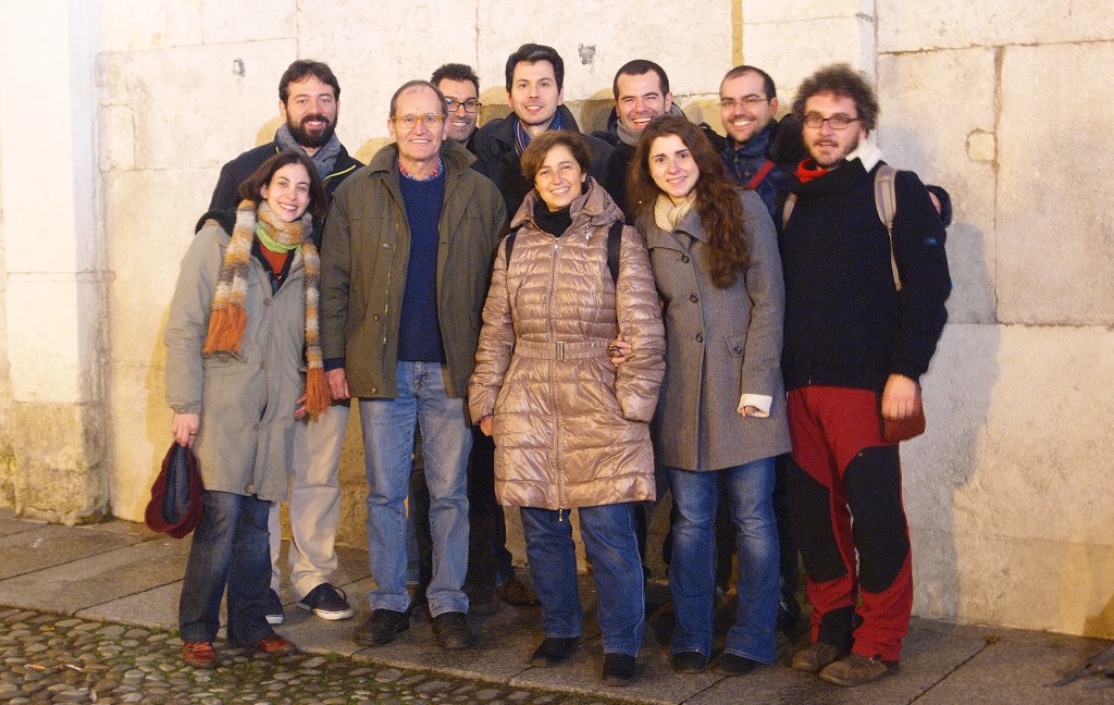
Welcome to the website of the Nanostructures Modelling Group

Our research activities are mainly centered on the development of theoretical and computational methods for the study of the structural, electronic and optical properties of semiconductor systems, in particular at the nanoscale. We use atomistic approaches, such as ab-initio DFT based methods, empirical approaches based on pseudopotentials (EPM), tight binding, classical interatomic potentials, valence force fields and molecular dynamics simulations, to study ground and excited state properties of low-dimensional and nanostructured materials. Multiscale and hybrid methods are also developed in our group.
The semiconductor nanostructured systems studied in our group are of interest for advanced applications, such as optoelectronic devices (lasers, detectors), energy harvesting (solar cells), sensoring (bio-nano-sensors), quantum computation (single photon emitters, spintronics).
Our activities are mainly developed at the University of Modena and Reggio Emilia and at the S3 national research centre of CNR-INFM, in collaboration with a number of national and international research groups.
If you want to know more about research, people, or opportunities at the Nanostructures Modelling Group, please visit our website and do not hesitate to contact us for any questions.

