April 2013 A publication within the European NASCENT collaboration on Silicon Tandem Solar Cells has been published
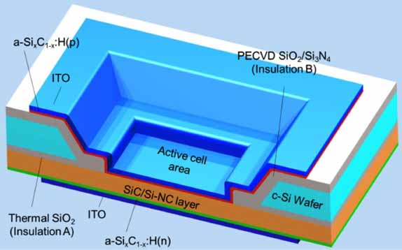
Silicon nanocrystals from high-temperature annealing: Characterization on device level Author(s): Löper, P.; Canino, M.; Lopez-Vidrier, J.; Schnabel, M.; Schindler, F.; Heinz, F.; Witzky, A.; Bellettato, M.; Allegrezza, M.; Hiller, D.; Hartel, A.; Gutsch, S.; Hernandez, S.; Guerra, R.; Ossicini, S.; Garrido, B.; Janz, S.; Zacharias, M. Silicon nanocrystals (Si NCs) embedded in Si-based dielectrics provide a Si-based high band gap material (1.7 eV) and enable the construction of all-crystalline Si tandem solar cells. However, Si nanocrystal formation involves high-temperature annealing which deteriorates the properties of any previously established selective contacts. The inter-diffusion of dopants during high-temperature annealing alters Si NC formation and limits the built-in voltage. Furthermore, most devices presented so far also involve electrically active bulk Si and therefore do not allow a clear separation of the observed photovoltaic effect of the nanocrystal layer from that of the bulk Si substrate. A membrane route is presented for nanocrystal based p–i–n solar cells to overcome these limitations. In this approach, the formation of both selective contacts is carried out after high-temperature annealing and therefore not affected by the latter. p–i–n Solar cells are investigated with Si NCs embedded in silicon carbide in the intrinsic region. Device failure due to damaged insulation layers is analyzed by electron- and light beam induced current measurements. Open-circuit voltages of 176 mV are shown for the NC layer. An optical model of the device is presented for improving the cell current. Comparison of the optical limit and the measured short circuit current demonstrates that the device is governed by recombination within the absorber layer.